Intel’s latest Core Ultra 9 285K, priced at $589, takes the spotlight as the flagship processor in the new Arrow Lake’ Core Ultra 200S series. Featuring 24 cores within a cutting-edge chiplet architecture, this CPU introduces a host of advanced technologies, including 3D Foveros packaging, support for the new DDR5 CUDIMM memory, and Intel’s first-ever dedicated AI engine integrated into a desktop chip. Despite these innovations, our gaming benchmarks revealed Arrow Lake's performance struggles to surpass Intel’s own Raptor Lake Refresh processors, let alone compete with AMD’s top-performing Zen 4 X3D CPUs.
Intel claims the Arrow Lake architecture achieves a 150W reduction in system power consumption during gaming, along with a 20% improvement in multi-threaded performance and a 5% gain in single-thread performance over the previous generation. While these benefits improve efficiency and productivity, they fall short in delivering meaningful generational gaming advancements. Across our 14-game test suite, the gaming performance lagged behind expectations, even as Intel maintained an edge in power efficiency and innovative core designs.
The launch comes amid AMD’s Zen 5 Ryzen 9000 series, which, despite being more energy-efficient, brought modest generational improvements to gaming performance. However, AMD’s upcoming Ryzen 9000X3D lineup, expected early next month, promises to reclaim the crown for gaming supremacy. Intel’s Arrow Lake CPUs, while innovative in architecture and power efficiency, will likely face stiff competition in this segment.
One standout feature of Arrow Lake is its use of TSMC nodes for its chiplets (termed "tiles" by Intel), making it Intel’s first mainstream desktop chip entirely fabricated on external process technology. This shift, paired with a radical redesign of CPU cores—abandoning Hyper-Threading and integrating E-core clusters among P-cores—aims to drastically reduce power consumption and create quieter, cooler PCs. While these innovations mark an exciting step forward, their gaming performance trade-offs may give enthusiasts pause in choosing Intel’s newest offering.
Intel Core Ultra 9 285K Pricing & Specifications
Intel has officially retired its generational branding, ending with the 14th-Gen family, and instead adopted the ‘Core Ultra’ naming convention already used in its mobile lineup. For desktop CPUs, the ‘S’ suffix now distinguishes these models. Additionally, the series begins at ‘200S’ rather than continuing sequentially from the previous generation’s numbering, so you didn’t miss a generation—this is just another quirk of Intel's evolving branding strategy.
The new Core Ultra desktop series features five Arrow Lake SKUs across the Ultra 9, Ultra 7, and Ultra 5 families, offering processors with 24, 20, and 14 cores, respectively. While the core counts match their prior-gen counterparts, Intel has dropped Hyper-Threading from the Performance cores (P-cores), resulting in lower total thread counts. Despite this, Intel claims—and our testing confirms—enhanced multi-threaded performance, achieved through architectural improvements and increased power efficiency.
The lineup includes Intel's standard overclockable K-series models and KF-series options for Core Ultra 7 and Ultra 5 processors, which omit integrated graphics. However, there is no KF version of the flagship Ultra 9 285K yet, leaving room for speculation about a possible future release.
This rebranding marks a significant shift for Intel, aiming to align its desktop and mobile naming strategies while introducing new architectural advancements like chiplet designs and integrated AI engines. Whether this fresh approach resonates with consumers remains to be seen, but the streamlined naming and focus on performance gains signal a bold step forward.
Intel’s Core Ultra 9 series debuts with the Arrow Lake processors, maintaining competitive pricing while introducing several notable changes. The flagship Ultra 9 285K is priced at $589, the same as the previous-gen Core i9-14900K. Meanwhile, the Ultra 7 265K launches at $394—a $15 reduction compared to the Core i7-14700K—and the Ultra 5 245K comes in at $309, a modest $10 decrease from the prior-gen Core i5-14600K.
Performance Adjustments
Intel has adjusted clock speeds, a trade-off tied to its transition to TSMC's N3B process node:
- The Ultra 9 peaks at 5.7 GHz, a 300 MHz reduction from the previous-gen’s 6 GHz boost clock.
- Ultra 7 and Ultra 5 see 100 MHz reductions in boost clocks but gain higher P-core base clocks by 500 to 700 MHz.
- E-cores enjoy boost clock improvements of 200 to 600 MHz and base clock increases of 600 MHz to 1 GHz, depending on the model.
Despite these reductions in peak clock speeds, multi-threaded workloads benefit from the architecture's refined performance, optimized power delivery, and increased thermal headroom.
Power and Thermal Changes
Arrow Lake introduces power optimizations while maintaining competitive TDP:
- Ultra 9 and Ultra 7 have an MTP of 250W, 3W lower than Raptor Lake.
- The Ultra 5 drops to 159W, saving 22W compared to its predecessor.
- Intel claims up to 40% lower power consumption during regular workloads while raising the maximum CPU temperature (TJMax) to 105°C, 5°C higher than previous mainstream processors.
Connectivity and Graphics
Arrow Lake processors support 24 PCIe 5.0 lanes and 20 PCIe 4.0 lanes from the chipset. All chips feature the Xe-LPG iGPU with:
- Four Xe cores at 2.0 GHz for Ultra 9 and Ultra 7.
- 1.9 GHz for Ultra 5.
While the iGPU promises twice the performance of the 14th-gen GPUs, its relevance remains limited for gaming PCs, as most users will rely on discrete GPUs.
AI and NPUs
Arrow Lake includes an NPU engine for AI acceleration, delivering 13 TOPS of INT8 throughput, the same as Meteor Lake. This falls short of Microsoft’s 40+ TOPS requirement for advanced AI features like Copilot+, but Intel prioritized optimizing die space for cores and cache over a more powerful NPU. For those needing AI compute, even budget GPUs like the RTX 4060 offer vastly superior AI capabilities.
Socket and Compatibility
Arrow Lake uses the new LGA 1851 socket, making it incompatible with earlier motherboards. Most existing coolers should work with appropriate mounting hardware, though this might vary by vendor. Intel’s commitment to LGA 1851 for future generations remains uncertain, with potential indications of a Core Ultra 2000S Refresh, suggesting this could be a single-generation socket.
Summary
With competitive pricing, improved efficiency, and meaningful updates to core and power architecture, Arrow Lake processors deliver balanced performance for desktop PCs. However, the reduced peak clock speeds and reliance on legacy iGPU and NPU designs may limit appeal for enthusiasts seeking the latest innovations. Whether Intel's focus on efficiency over sheer performance will resonate with consumers remains to be seen.
CUDIMMs and Memory Support
Arrow Lake processors support up to 192GB of DDR5 memory and offer two different base speeds with DDR5 CUDIMMs (Clocked Unbuffered DIMMs) being a notable new option. These CUDIMMs incorporate an integrated clock driver (ckd) that enhances the stability of high-frequency memory by amplifying the signal, stabilizing the data eye without adding extra latency. This is a more cost-effective and simpler design compared to fully-buffered registered DIMMs, which have a more complex redriver that adds latency.
Intel claims that CUDIMMs offer significantly higher overclocking headroom, with DDR5-8000 being the optimal target for high-frequency performance in Gear 2 mode. This advancement should also make it possible to use lower-quality DRAM ICs in high-speed kits and simplifies the design of **high-end memory DIMMs, potentially reducing costs. However, CUDIMMs may carry a price premium, and motherboards supporting them could be more expensive, so it’s important to evaluate the total cost when considering this option.
Intel also continues to support standard DDR5 memory, but at lower base speeds (up to DDR5-5600**) compared to the CUDIMMs. Both memory types are overclockable, and while ECC (Error-Correcting Code) memory is supported by Arrow Lake, it will only be available on enterprise-focused W-series motherboards, not on consumer platforms.
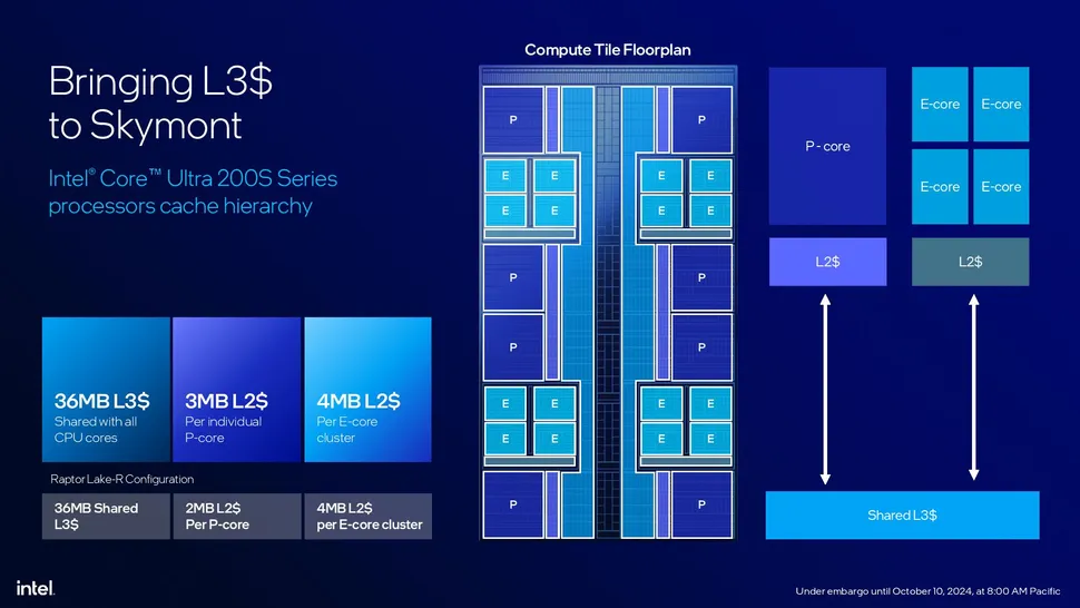
Intel Arrow Lake Ultra 200S Architecture
Arrow Lake represents Intel's debut into a disaggregated architecture, where distinct compute and I/O functionalities are divided into separate dies. This architecture is referred to by Intel as a ‘tiled’ architecture, while the rest of the industry commonly uses the term chiplet architecture.
Intel differentiates its tiled design by emphasizing its use of advanced packaging, which facilitates parallel communication between the tiles. This approach is claimed to offer superior performance and energy efficiency compared to the serial interfaces often employed in standard packaging. Despite Intel’s branding distinction, other processors utilizing advanced packaging techniques are still generally described as chiplet-based, making the terms largely interchangeable in practical contexts.
(image credit: intel)
Instead of adopting the newer Lunar Lake package design, Arrow Lake continues with a structure akin to its five-tile Meteor Lake laptop processors. However, Intel has integrated the Lion Cove P-core and Skymont E-core microarchitectures in the compute tile, replacing the Redwood Cove and **Crestmont cores from Meteor Lake.
Arrow Lake's design employs a diverse set of process nodes across its components:
- Compute Tile: Fabricated on TSMC's N3B process node, leveraging cutting-edge advancements for core processing.
- GPU Tile: Built on TSMC's N5P node, ensuring powerful and efficient graphics performance.
- SoC and I/O Tiles: Manufactured using TSMC's N6 process, balancing efficiency and functionality.
- Base Tile: Constructed with Intel's 1227.1 process node (22nm FinFET), serving as the foundational layer for the package.
Intel employs Foveros 3D packaging technology to stack and integrate these tiles onto the base tile. Additionally, the design includes two ‘dummy’ filler tiles, which contribute to the processor's mechanical rigidity without adding functional components. This layered approach exemplifies Intel's strategy of blending in-house and outsourced manufacturing to deliver innovative solutions.
Intel reports that the Arrow Lake processors contain 17.8 billion transistors, distributed over a total die area of 243mm². However, the inclusion of filler tiles in this measurement and the use of varied process nodes make it difficult to draw definitive conclusions about the chip's transistor density.
One of Intel’s design decisions was to split the memory controller and PHY into a separate I/O tile, allowing the high-performance 3nm transistors to be reserved for compute tasks, thereby improving yield efficiency. However, this architectural choice has led to increased memory latency, which appears to be a factor in the lower gaming performance observed in benchmarks.
Intel provides an option to overclock the tile-to-tile interface, which could potentially mitigate some of the latency penalties, but its impact remains untested. Below is key latency figures measured using AIDA and the Memory Latency Tool developed by the Chips and Cheese team, illustrating the trade-offs in Intel's innovative yet complex design approach.
Conclusion
The Intel Core Ultra 9 285K showcases notable improvements in productivity workloads, leveraging its advanced tiled architecture and newer microarchitectures to deliver impressive multi-threaded performance. However, when it comes to gaming, the processor falls short of its predecessor, the Core i9-14900K, due to increased memory latency and architectural trade-offs.
This performance gap positions AMD's competing Zen 4 X3D chips as a better value for gaming enthusiasts, offering superior frame rates and smoother gameplay. Furthermore, the reduced pricing on the Core i9-14900K makes it a strong contender within Intel's own lineup, providing a compelling alternative for users seeking gaming-focused performance at a lower cost.
Intel Core Ultra 9 285K Pros and Cons
Pros
- Strong Productivity Performance: Excels in multi-threaded workloads, making it ideal for content creators and professionals.
- Improved Power Efficiency: Up to 40% reduction in package power during typical workloads, resulting in quieter and cooler operation.
- CUDIMM Memory Support: Enables stable high-speed memory configurations with reduced latency.
- Relaxed Cooling Requirements: Lower peak power draw and better efficiency make it easier to cool compared to prior generations.
- Higher Memory Overclocking Headroom: DDR5 CUDIMM compatibility allows for overclocking up to DDR5-8000, offering more flexibility for enthusiasts.
Cons
- High Pricing: At $589, it competes with more cost-effective options like AMD's Ryzen 7 9800X3D or even Intel's prior-gen Core i9-14900K.
- Gaming Performance Regression: Increased memory latency and architectural changes lead to performance dips in gaming compared to its predecessor.


Comments
Post a Comment